I could only do this assignment after thoroughly testing the Flipdot module for my final project. It might make more sense to read about the Electronics Design on the Final Project page.
I have decided to split my design into two, one board for the logic and one to address the rows of my display. This second board needs to have 32 MOSFETs and after consulting with Ahmed I decided to order it off of JLCPCB already fully assembled to save time.
Controller Board
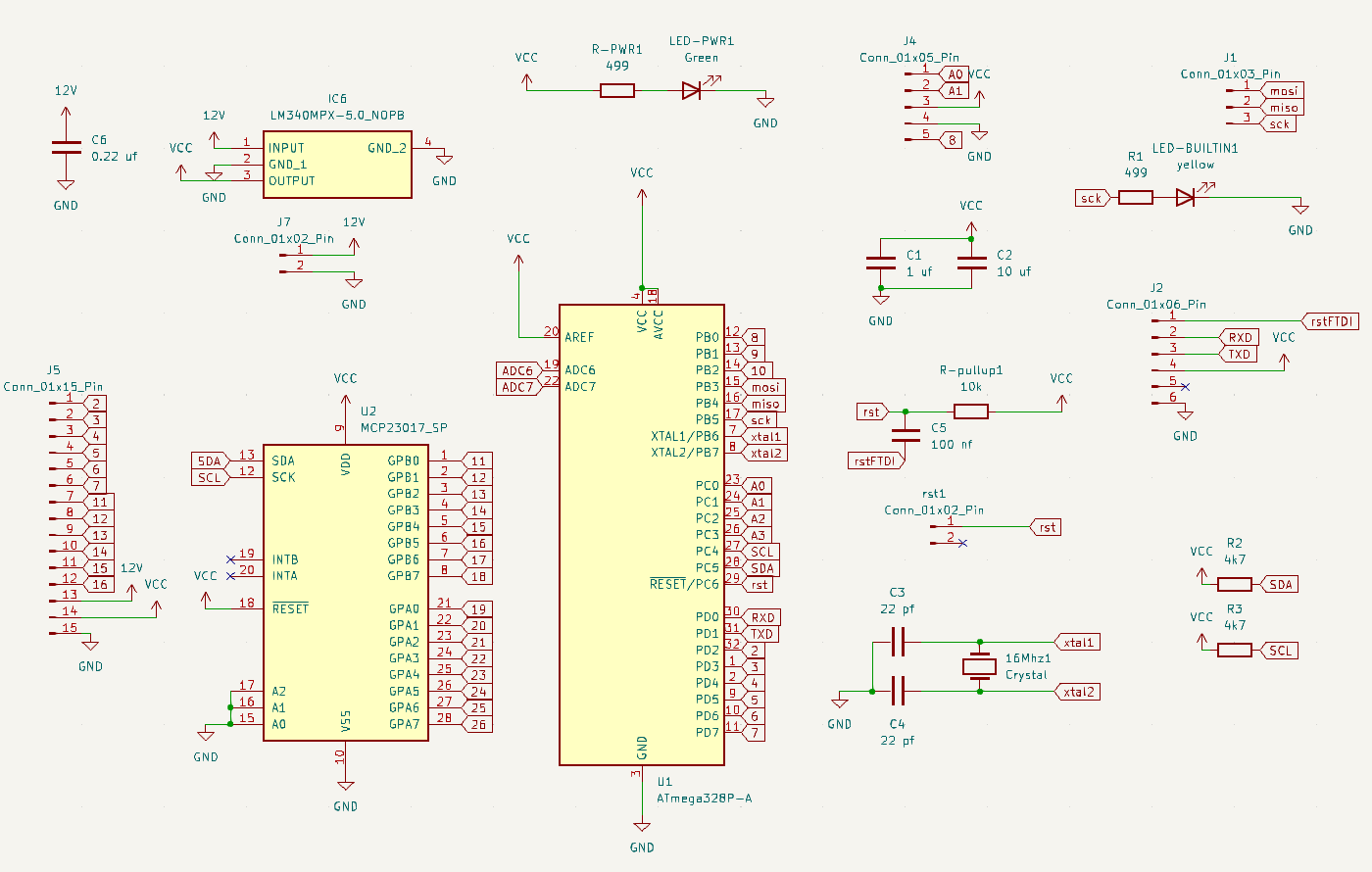 The controller board is going to do the computation and handle the logic of the whole project. It needs to connect to three external components:
- A Computer via the Serial to USB interface we built in Week 7
- The Joystick
- The Decoder Board
Another thing the controller board needs to handle is power. Since the dots need 12V to flip, the board uses a linear voltage regulator to step 12V down to 5V. This means that the 12V can be passed to the decoder board and the controller can use the stepped down 5V eliminating the necessity for the lab power supply.
The chip we are using for this class is the ATmega328P-A which has 9 digital pins. But my board needs more than that:
| Pin Count | Usage |
|---|---|
| 1 | Joystick Button |
| 6 | Custom Decoder Board |
| 6 | Chip on the Flipdot module |
| Because of this I elected to use a GPIO expander. This IC is addressed via I2C and provides 16 additional digital Pins. |
The full bill of material for this board can be found here (exported from KiCad Project):
Transclude of digiFabFinal.csv
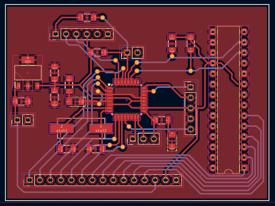 The routing for this board was pretty challenging, because of this I chose to use two layers, the front and the back of the board. This meant I had to use VIAs, but more on that in Manufacturing the Controller Board. But because of that I managed to fit all of my components very close together avoiding wasting too much material.
Decoder Board
My decoder board needs to do one thing: address the 32 pins for the rows of my display. I need to be able to have all the Reset pins unconnected or high and all the Set pins unconnected or GND. Then I have to be able to pull one specific Reset pin down to GND or one specific Set pin up to 12V.
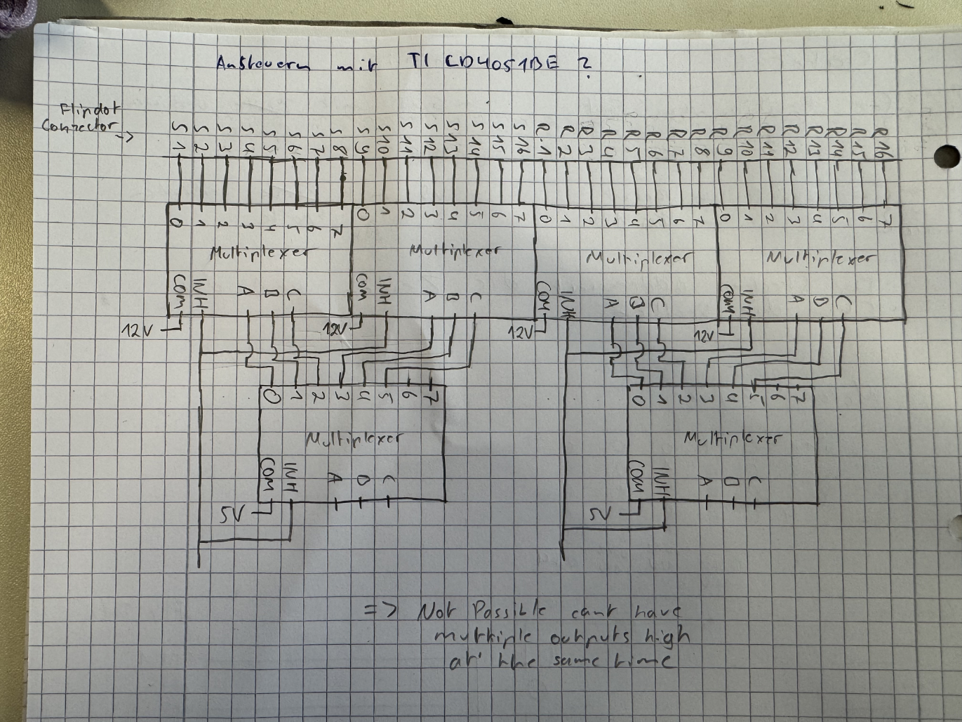 At first I decided I should create the board using six Multiplexers. This would allow me to address 32 pins and provide them with either GND or 12V. But with this design it is not possible to have multiple outputs high at the same time, which would be necessary for the Reset pins.
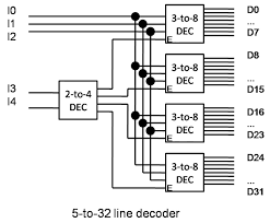 Then I found this graphic explaining how to create a 5 to 32 line decoder and decided that I would need to implement this logic if I wanted to address my display. This allows me to address all 32 pins individually and only uses 5 digital pins of the ATmega. I would need to have a MOSFET behind each output of the decoder but that is not a problem.
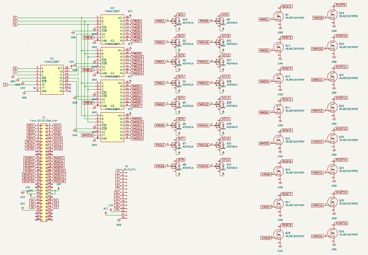 This is the design I came up with according to the diagram above. I am using five decoder ICs. Behind each output is a MOSFET, 16 are P-Channel and 16 are N-Channel. This allows me to address all 32 pins of the Flipdot display.
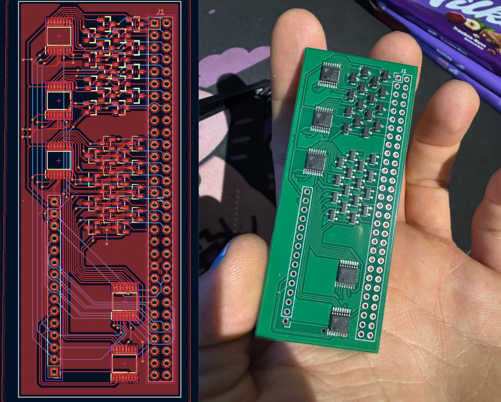 This is the resulting PCB, I also used two layers to make routing simpler and then ordered it off JLCPCB.